
EIRR21 Annual Research Day, June 2009. read more
Research
Sample results:
S. Cuddy, A. Reznik, J. A. Rowlands, F. Taghibakhsh "Effect of scintillator crystal geometry and surface finishing on depth of interaction resolution in PET detectors", Proceedings of SPIE, Physics of Medical Imaging, vol. 7622, March 2010.
F. Taghibakhsh, S. Cuddy, T. Rvachov, D. Green, A. Reznik, J. A. Rowlands, "Detectrs with Dual-Ended Readout by Silicon Photomultipliers for High Resolution Positron Emission Mammography Applications", 2009 IEEE Nuclear Science Symposium Conference Record, pp. 2821-2826, October 2009.
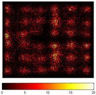
Detector flood-fill image obtained from a 6x6 crystal array coupled to a 4x4 silicon photomultiplier array.
This research explores capabilities of a-Si APS based x-ray imaging arrays to meet the requirements of emerging medical diagnostics modalities such as cone beam computed tomography and digital tomosynthesis (3D mammography). I successfully demonstrated direct x-ray detection using a-Si APS integrated with amorphous selenium x-ray photoconductor for high resolution x-ray imaging applications.
Sample results:
F. Taghibakhsh, K. S. Karim, G. Belev, S. O. Kasap, "X-Ray Detection using a Two-Transistor Amplified Pixel Sensor Array coupled to an a-Se X-Ray Photoconductor", IEEE Sensors Journal, vol. 9, no. 1, p. 51-56, January 2009.
F. Taghibakhsh, K. S. Karim, 'High Resolution Amplified Pixel Architectures for Large Area Digital Mammography Tomosynthesis', Proceedings of SPIE, Medical Imaging, vol. 6913, 69133R1-9, February 2008, (Honorable Mention Poster Award).
F. Taghibakhsh, K. S. Karim, 'Amplified Pixel Architectures for Low Dose Computed Tomography using Silicon Thin Film Technology', Proceedings of SPIE, Medical Imaging, vol. 6510, 65103w1-8, February 2007, (Honorable Mention Poster Award).

A bonded high resolution (100µm pixel pitch) 2T-APS test array coated with a-Se direct x-ray detector for performance evaluation
High Resolution Low dose Large Area Digital Imaging The objective of this research is to extend the amorphous silicon (a-Si) technology from switch-based pixel arrays towards pixel amplifiers to enable a-Si active pixel sensor (APS) array for large area medical x-ray imaging. Challenges are improving pixel resolution, gain and noise performance, as well as adaptability to the current state-of-the-art passive pixel sensor (PPS) based flat panel technology. My contribution to this field is development of a new generation of APS architecture based on switched-amplifier thin film transistors (TFTs).
Sample results:
F. Taghibakhsh, K.S. Karim, "Two-Transistor Active Pixel Sensor Readout Circuits in Amorphous Silicon Technology for High Resolution Digital Imaging Applications ", IEEE Transactions on Electron Devices, vol. 55, no. 8, pp. 2121-2128, August 2008.
F. Taghibakhsh, K. S. Karim, "Two-Transistor Active Pixel Sensor for High Resolution Large Area Digital X-ray Imaging", IEEE - IEDM International Electron Devices Meeting, pp. 1011-1014, December 2007.

Micrograph of a high-resolution (100µm pixel pitch) two-transistor APS array fabricated using a-Si TFTs.
a-Si TFT Integrated Sensors The objective of this research is to explore and develop alternative devices, circuits and processes for fabrication of a-Si integrated sensor arrays compatible with a-Si TFT fabrication technology.
Sample results:
F. Taghibakhsh, I. Khodami, K. S. Karim, Characterization of Short Wavelength Selective a-Si MSM Photoconductors for Large Area Digital Imaging, IEEE Transaction on Electron Devices, vol. 55, no. 1, pp. 337-342, Jan. 2008.
F. Taghibakhsh, K. S. Karim, 'Light Controlled Oscillator; A Pixel Architecture for Large Area Linear Digital Imagers', Proceedings of IEEE CCECE, pp. 1279-12-82, May 2008.

Micrograph of a light controlled oscillator thin film circuit. Both the sensor and its readout circuit are fabricated together in the same process.
Hot-Wire Deposited Silicon Thin Film Devices The objective of this research was to explore capabilities of hot-wire chemical vapor deposition (HW-CVD) in developing high-yield inexpensive large area fabrication processes specially on flexible substrates. Compared to plasma enhanced CVD, HW-CVD is easily scalable to very large areas, simply adaptable to roll-to-roll deposition, and a-Si TFTs deposited using HW exhibit improved stability.
Sample results:
F. Taghibakhsh, M. M. Adachi, K. S. Karim, "Hot-wire Deposited Nanocrystalline Silicon TFTs on Plastic Substrates", Proceedings of Material Research Society, vol. 989, A20-04, April 2007.
F. Taghibakhsh, K. S. Karim, A. Madan, "Low leakage a-Si:H Thin Film Transistor Deposited on Glass Using Hot-wire Chemical Vapor Deposition", Journal of Vacuum Science & Technology A: Vacuum, Surfaces, and Films, Volume 24, Issue 3, pp. 866-868, (2006)
F. Taghibakhsh, K. S. Karim, "Hot-wire CVD a-Si TFTs on Plastic Substrate", Proceedings of Material Research Society , vol. 910, A18-02, April 2006.

Glowing graphite filament inside the HW deposition chamber.

A low voltage inverter gate fabricated using HW deposited nc-Si on a Kapton plastic sheet.
Charge-Gated Thin Film Transistor A CG-TFT or charge gated thin film transistor is a TFT with two gates: a normal voltage gate and a charge gate. The device si normally operated using its voltage gate, however, the amount of charge deposited on the charge gate also modulates the current in the channel.
Reference:
F. Taghibakhsh, K. S. Karim, "Charge-Gated Thin Film Transistor for High Resolution Digital Imaging", IEEE Electron Device Letters, vol. 29, no. 8, pp. 859-862, August 2008.

The Field Effect Diode The objective of this research was to simulate the electrical characteristics a novel device proposed by Prof. Farshid Raisi: the field effect diode (FED). Unlike regular silicon devices, FED is an SOI device and requires compensated silicon (semi-intrinsic) for proper operation. Structurally it is similar to a MOSFET with differently doped drain and source (one p+, the other n+), having two gates over an intrinsic channel. Such a device finds applications in RF signal modulation, multilevel logics, and output stages of ICs.
Sample results:
F. Taghibakhsh, F. Raisi, "A Numeric Simulation of the Static Volt-Ampere Characteristics of the Field Effect Diode", Proceedings of the The 11th Iranian Conference on Electrical Engineering, vol. 1, pp. 542-547, May 2003.
F. Taghibakhsh, "The Field effect Diode", Semiconductor Device Research Symposium, pp. 236 in abstract book, December 2003.

2D simulation results of distribution of the electrostatic potential, density of electrons and holes in a revese biased FED.
Porous Polycrystalline Zinc Oxide Devices The objective of this research was to characterize an electrophoretic deposition (EPD) process for forming a highly porous polycrystalline zinc oxide thick film, and develop a fabrication process to integrate the semiconductor thick film with the heater substrate for chemical sensing applications. Challenges such as reproducibility of the EPD process and formation of an electrical insulating layer between the metallic substrate (the heater) and the semiconducting thick film (the sensor) were dealt. This was my MSc thesis.
Sample results:
F. Hossein Babaei, F. Taghibakhsh, "Electrophoretically Deposited Zinc Oxide Resistive Thick Film Gas Sensors", IEE Electronics Letters Journal, vol. 36, no. 21, pp. 1815-16, August 2000.
F. Hossein-Babaei, F. Taghibakhsh,"A new method for fabrication of resistive thick film gas sensors", 103rd Annual Meeting of the American Ceramic Society, pp. 106 in abstract book, April 2001.

Highly porous ZnO polycrystalline film for chemical sensing applications. The ceramic film was deposited using electrophoresis and sintered at 1100 ºC. The average grain size is 400 nm.
Contact Information (go to updated contact information):
Imaging Research - S634 B,
Sunnybrook Health Sciences Center,
2075 Bayview Avenue
Toronto, Ontario,
M4N 3M5
Phone: 416-480-6100, ext. 3274
Fax: 416-480-5714
![]()